We provide custom printed circuit board design and layout for smart Home & IOT,Power electronics, Industry electronics,consumer electronics etc for a variety of electronic systems and fields of application.
You might already have design schematics created and require a PCB layout from them, or you might be looking to improve and optimize your existing design for cost-effective assembly. We can help you build PCB designs, including high speed PCB design from scratch, as well as provide technology consulting services to solve any technical complexities you might have.
A list of our tools :
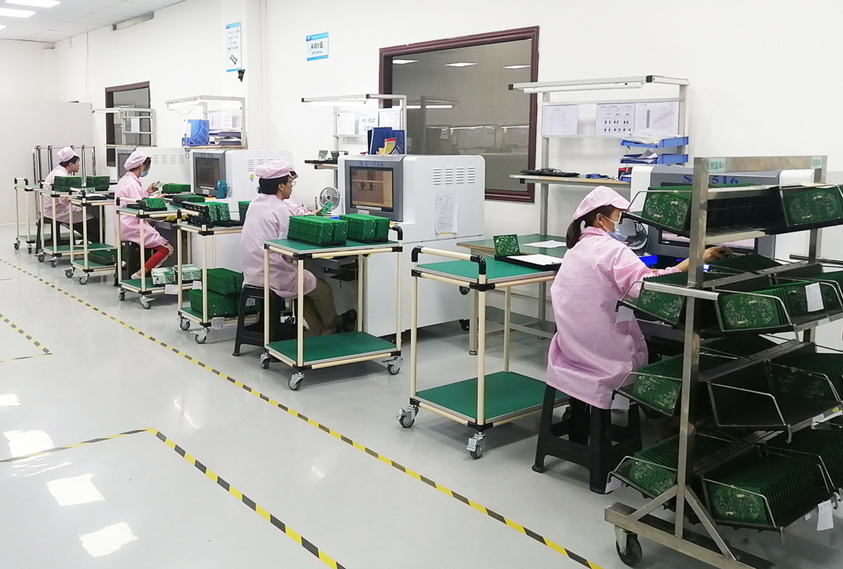
Visual inspection following IPC criteria HD Camera
2D AOI (Automatic Optical Inspection)
Flying probe test
X-ray inspection
Functional test with dedicated test bench and bay (Custom, National Instrument)
DIEL test Isolation
Burn-in (cycle defines -30°C to +150°C with power supply)
Ionic decontamination
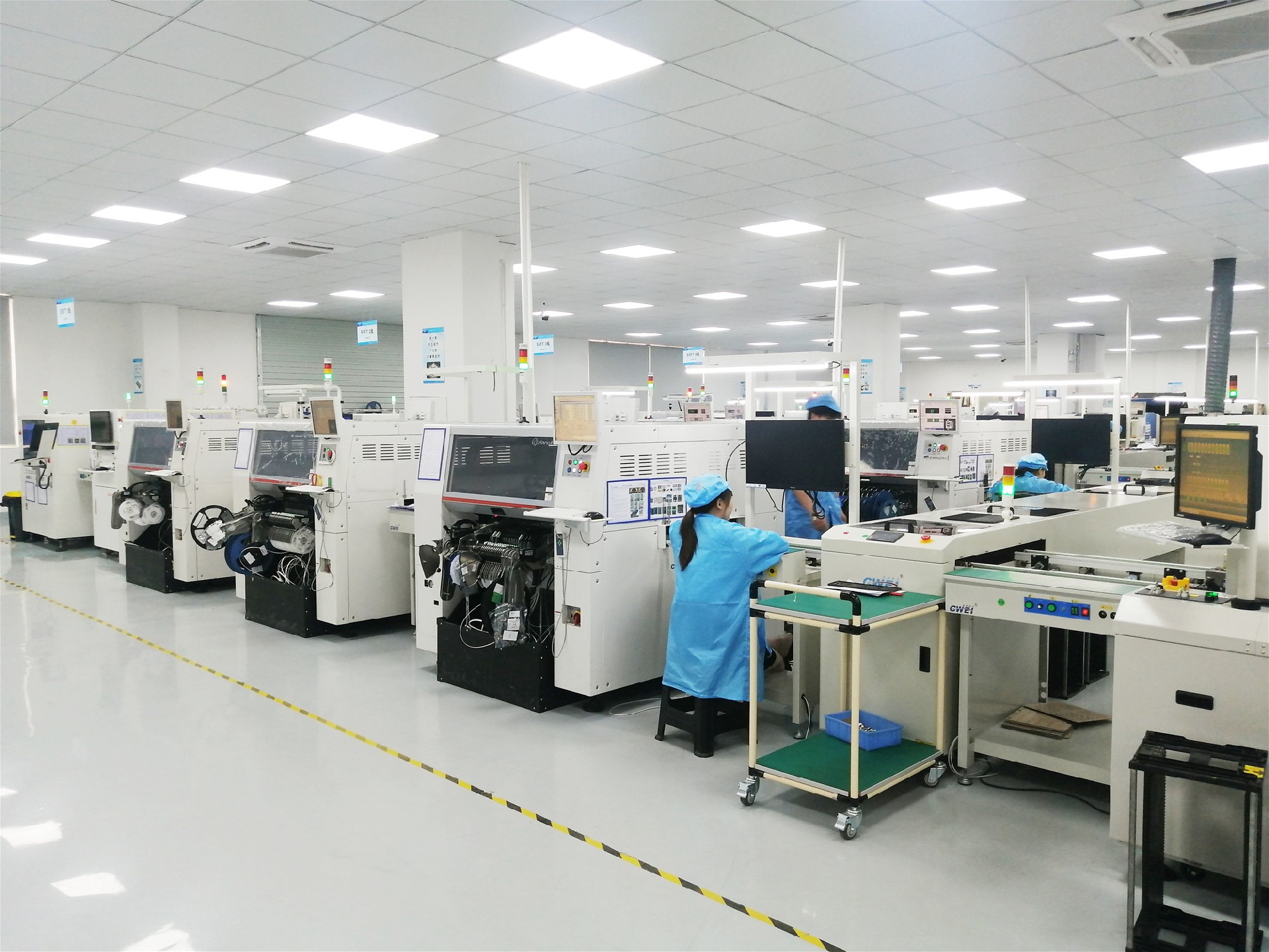
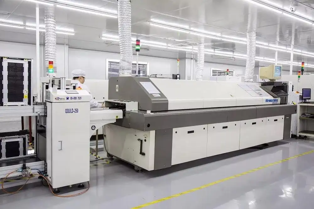
We have 6 SMT lines, fully automated with :
PCB Stacker/Destacker
Removing/placing solder paste with 2D inspection
Placement machines Pick and Place
Reflow oven
X-ray inspection
The products are qualified from prototypes to mass production, with the same recommendations and the same machines.
For your PCB assembly projects, we can take care of your component sourcing according to your Bill of Material (BOM), so that you don’t have to worry about checking and comparing with multiple sources on quantities and prices.
We work with all major global distributors such as Digikey, Mouser, Element 14, Future etc., and also with China local authorized distributors, in this way we can deliver reliability and traceability components assembled on board ( or not assembled ) to your hand.
In electronics, we're talking about soldering which uses temperatures below 450°C.
Wave soldering : ROHS tin or lead bath
Selective wave soldering : wave “finger” by a conventional soldering head driven in X, Y, Z
With the latter, we use an automated point to point soldering technique, replacing the soldering iron.
Our soldering process is RoHs qualified, but we also keep the leaded process for certain activities.
Our soldering is carried out in an inert atmosphere with nitrogen supply that reduces the level of oxygen to improve the wettability of the solder.
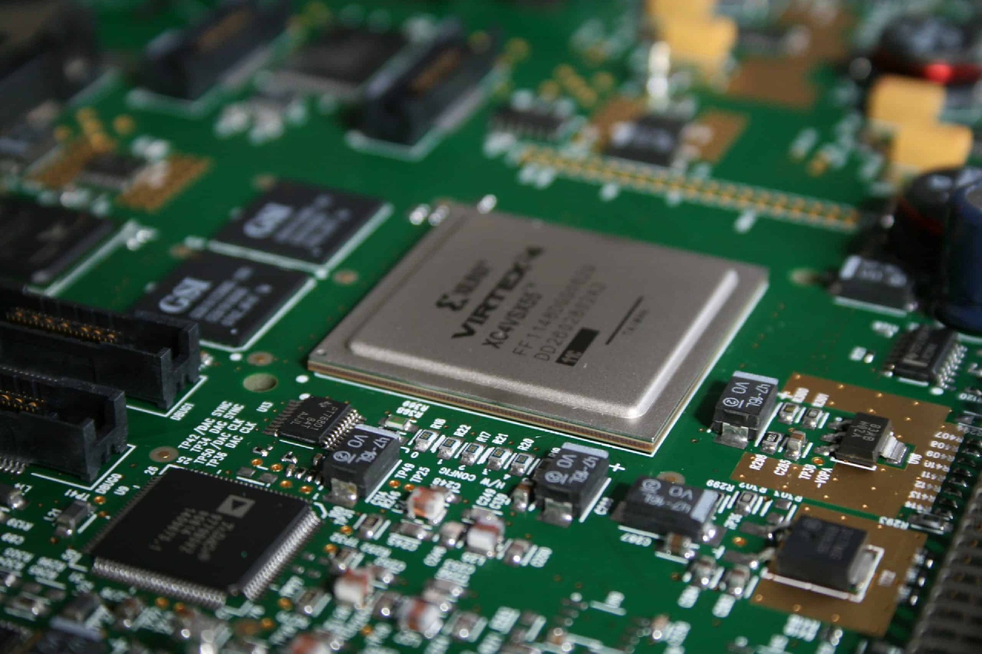
Technological capabilities of SMD assembly :
Minimal size of discrete component 0201,
integrated circuits and connectors - minimal pitch 0.35mm,
uBGA, BGA, QFP, MLF, PLCC
Max.PCB size : 450*500mm
Part thickness: 0.5mm ≤T ≤ 3mm
Max Parts size assembly by machine: SMD ≤ 200*125mm
PCB type: Rigid PCB,flex pcb, Semi-flex pcbs